Maharashtra State Board 12th Physics Solutions Chapter 16 Semiconductor Devices
1. Choose the correct option
i.
In a BJT, the largest current flow occurs
(A) in the emitter
(B) in the collector
(C) in the base
(D) through CB junction.
Answer:
(A) in the emitter
ii.
A series resistance is connected in the Zener diode circuit to
(A) properly reverse bias the Zener
(B) protect the Zener
(C) properly forward bias the Zener
(D) protect the load resistance.
Answer:
(A) properly reverse bias the Zener
iii.
An LED emits visible light when its
(A) junction is reverse biased
(B) depletion region widens
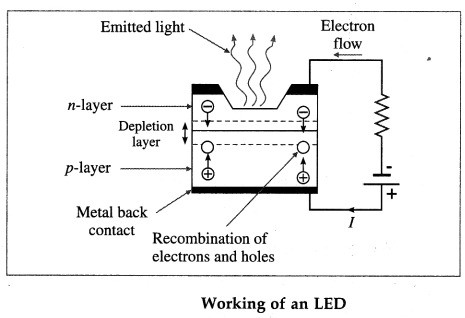
(C) holes and electrons recombine
(D) junction becomes hot.
Answer:
(C) holes and electrons recombine
iv.
Solar cell operates on the principle of
(A) diffusion
(B) recombination
(C) photovoltaic action
(D) carrier flow.
Answer:
(C) photovoltaic action
v.
A logic gate is an electronic circuit which
(A) makes logical decisions
(B) allows electron flow only in one direction
(C) works using binary algebra
(D) alternates between 0 and 1 value.
Answer:
(A) makes logical decisions
2 Answer in brief.
i.
Why is the base of a transistor made thin and is lightly doped?
Answer:
The base of a transistor is lightly doped than the emitter and is made narrow so that virtually all the electrons injected from the emitter (in an npn tran-sistor) diffuse right across the base to the collector junction without recombining with holes. That is, the base width is kept less than the recombination distance. Also, the emitter is much heavily doped than the base to improve emitter efficiency and common-base current gain a.
ii.
How is a Zener diode different than an ordinary diode?
Answer:
A Zener diode is heavily doped-the doping con-centrations for both p- and n-regions is greater than 1018 cm-3 while those of an ordinary diode are voltage (PIV) of an ordinary diode is higher than a Zener diode and the breakdown occurs by impact ionization (avalanche process). Their I-V characteristics are otherwise similar.
iii.
On which factors does the wavelength of light emitted by a LED depend?
Answer:
The intensity of the emitted light is directly propor-tional to the recombination rate and hence to the diode forward current. The colour of the light emitted by an LED depends on the compound semiconductor material used and its composition (and doping levels) as given below :
Table: Typical semiconductor materials and emitted colours of LEDs
Material | Emitted colour(s) |
Gallium arsenide (GaAs), Indium gallium arsenide phosphide (InGaAsP) | Infrared |
Aluminum gallium arsenide (AlGaAs) | Deep red, also IR laser |
Indium gallium phosphide (InGaP) | Red |
Gallium arsenide phosphide (GaAsP), aluminum indium gallium phosphide (AlInGaP) | Orange, red or yellow |
Gallium phosphide (GaP) | Green or yellow |
Aluminium gallium phosphide (AlGaP), zinc selenide (ZnSe), zinc selenide telluride (ZnSeTe), nitrogen impregnated gallium phosphide (GaP:N) | Green |
Indium gallium nitride (InGaN), gallium nitride (GaN), sine sulphide (ZnS) | Blue and violet Longer wave lengths (green and yellow) are obtained by increasing the indium (In) content. Phosphor encapsulation produce white light. |
Aluminium gallium nitride (AlGaN) | Ultraviolet |
iv.
Why should a photodiode be operated in reverse biased mode?
Answer:
A photodiode is operated in a reverse biased mode because as photodetector or photosensor, it must conduct only when radiation is incident on it. In the reverse biased mode, the dark current for zero illumination is negligibly small—of the order of few picoamperes to nanoamperes. But when illuminated, the photocurrent is several orders of magnitude greater.
v.
State the principle and uses of a solar Cell.
Answer:
A solar cell is an unbiased pn-junction that converts the energy of sunlight directly into electricity with a high conversion efficiency.
Principle : A solar cell works on the photovoltaic effect in which an emf is produced between the two layers of a pn-junction as a result of irradiation.
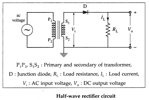
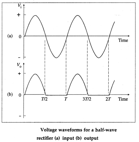
Thus, the diode conducts only during one-half of the input cycle and thus acts as a half-wave rectifier. The intermittent output voltage V0has a fixed polarity but changes periodically with time between zero and a maximum value. ILis unidirectional. Above figure shows the input and output voltage waveforms.
The pulsating dc output voltage of a half-wave rectifier has the same frequency as the input.
The circuit used in a dc power supply to remove the ripple is called a filter. A filter circuit can produce a very smooth waveform that approximates the waveform produced by a battery. The most common technique used for filtering is a capacitor connected across the output of a rectifier.
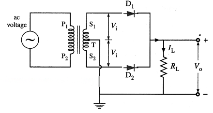
Working : During one half cycle of the input, terminal S1of the secondary is positive while S2is negative with respect to the ground (the centre-tap T). During this half cycle, diode D1is forward biased and conducts, while diode D2is reverse biased and does not conduct. The direction of current ZLthrough RLis in the sense shown.
During the next half cycle of the input voltage, S2 becomes positive while S, is negative with respect to T. Diode D2 now conducts sending a current IL through RL in the same sense as before. Dt now does not conduct. Thus, the current through RL flows in the same direction, i.e., it is unidirectional, for both halves or the full-wave of the input. This is called full-wave rectification.
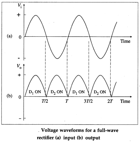
The output voltage has a fixed polarity but varies periodically with time between zero and a maximum value. Above figure shows the input and output voltage waveforms. The pulsating dc output voltage of a full-wave rectifier has twice frequency of the input.
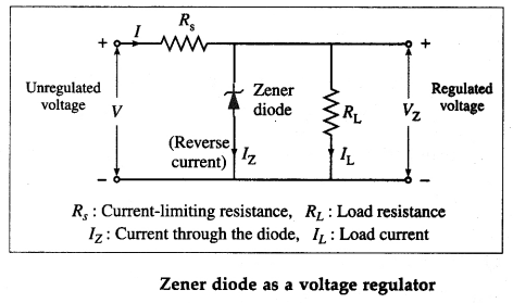
As the load current (I) or supply voltage (V) changes, the diode current (7Z) adjusts itself at constant VZ. The excess voltage V-VZappears across the series resistance Rs.
For constant supply voltage, the supply current I and the voltage drop across Rsremain constant. If the diode is within its regulating range, an increase in load current is accompanied by a decrease in Iz at constant VZ.
Since the voltage across RLremains constant at VZ, the Zener diode acts as a voltage stabilizer or voltage regulator.
The typical forward voltage at room temperature with a current of around 1 mA is around 0.6 V.
In the reverse bias condition the Zener diode is an open circuit and only a small reverse saturation current flows as shown with change of scale. At the reverse breakdown voltage there is an abrupt rapid increase in the current-the knee is very sharp, followed by an almost vertical increase in current. The voltage across the Zener diode in the breakdown region is very nearly constant with only a small increase in voltage with increasing current. There is a minimum Zener current, IZ(min), that places the operating point in the desired breakdown region. At some high current level, IZM, the power dissipation of the diode becomes excessive beyond which the diode can be damaged.
Zener diode characteristics
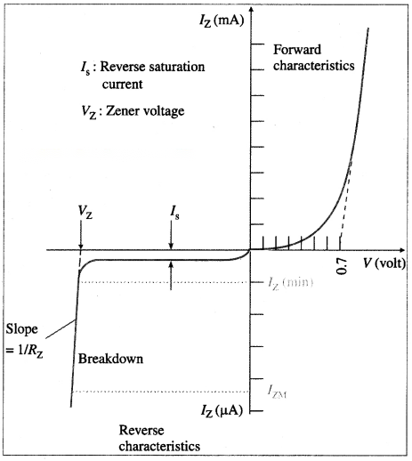
The I-V characteristics of a Zener diode is not totally vertical in the breakdown region. This means that for slight changes in current, there will be a small change in the voltage across the diode. The voltage change for a given change in current is the resistance RZof the Zener diode.
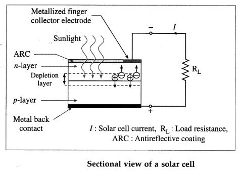
Consider light of frequency v incident on the pn-junction such that the incident photon energy hv is greater than the band gap energy EG of the semiconductor. The photons excite electrons from the valence band to the conduction band, leaving vacancies or holes in the valence band, thus generating electron-hole pairs.
The photogenerated electrons and holes move towards the n side and p side, respectively. If no external load is connected, these photogenerated charges get collected at the two sides of the junction and give rise to a forward photovoltage. In a closed- circuit, a current I passes through the external load as long as the solar cell is exposed to sunlight.
A solar cell module consists of several solar cells connected in series for a higher voltage output. For outdoor use with higher power output, these modules are connected in different series and parallel combinations to form a solar cell array.
[Note : Currently most of the crystalline solar cells are p-type as described above. This is because of a lower cost of production of p-type. But performance wise, n-type solar cells (a thin p-layer over an n-type substrate by doping with suitable acceptor impurity) can give much better efficiency compared to p-type solar cells.]
The area of the p-layer defines the photodiode active area. An ohmic contact pad is deposited on the active area. The rest of the active area is left open with a protective antireflective coating of silicon nitride to minimize the loss of photons. The nonactive area is covered with an insulating opaque SiO2coating.
Depending on the required spectral sensitivity, i.e., the operating wavelength range, typical photodiode materials are silicon, germanium, indium gallium arsenide phosphide (InGaAsP) and indium gallium arsenide (InGaAs), of which silicon is the cheapest while the last two are expensive.
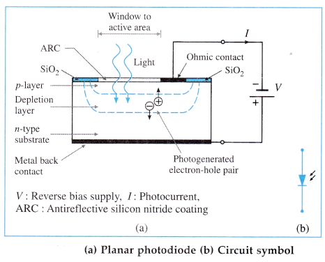
Working : The band gap energy of silicon is EG= 1.12 eV at room temperature. Thus, photons or particles with energies greater than or equal to 1.12 eV, which corresponds to 110 nm, can transfer electrons from the valence band into the conduction band.
A photodiode is operated in the reverse bias mode which results in a wider depletion region. When operated in the dark (zero illumination), there is a reverse saturation current due solely to the thermally generated minority charge carriers. This is called the dark current. Depending on the minority carrier concentrations, the dark current in an Si photodiode may range from 5 pA to 10 nA.
When exposed to radiation of energy hv ≥ EG(in the range near-UV to near-IR), electron-hole pairs are created in the depletion region. The electric field in the depletion layer accelerates these photogenerated electrons and holes towards the n side and p side, respectively, constituting a photocurrent l in the external circuit from the p side to the n side. Due to the photogeneration, more charge carriers are available for conduction and the reverse current is increased. The photocurrent is directly propor-tional to the intensity of the incident light. It is independent of the reverse bias voltage.
[Notes : Typical photodiode materials are :
(1) silicon (Si) : low dark current, high speed, good sensitivity between ~ 400 nm and 1000 run (best around 800 nm-900 nm)
(2) germanium (Ge) : high dark current, slow speed, good sensitivity between ~ 900 nm and 1600 nm (best around 1400 nm-1500 nm)
(3) indium gallium arsenide phosphide (InGaAsP) : expensive, low dark current, high speed, good sensitivity between ~ 1000 nm and 1350 nm (best around 1100 nm- 1300 nm)
(4) indium gallium arsenide (InGaAs): expensive, low dark current, high speed, good sensitivity between ~ 900 nm and 1700 nm (best around 1300 nm-1600 nm],
Explanation/Uses :
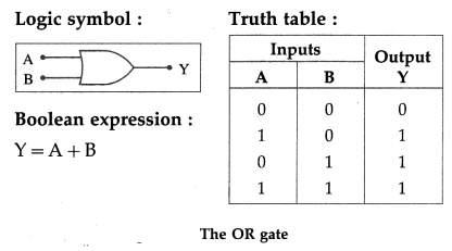
Any digital computation process consists in performing a sequence of arithmetical operations on the data of the problem. At each stage in the computation, the nature of the operation to be performed is decided partly by the pre-determined program and partly by the outcome of earlier stages in the process. We therefore need switches with multiple inputs to perform logical operations, i.e., the outputs of these switches are determined in specified ways by the condition (binary state) of their inputs. These arrangements are known as logic gates, and mostly they are extension of a simple transistor switch.
(1) Boolean expression : An equation expressing a logical compound statement in Boolean algebra is called a Boolean expression. A Boolean expression for a logic gate expresses the relation between input(s) and output of a logic gate.
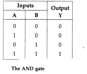
(2) Truth table : The table which shows the truth values of a Boolean expression for a logic gate for all possible combinations of its inputs is called the truth table of logic gate.
The truth table contains one row for each input combination. Since a logical variable can assume only two possible values, 0 and 1, there are 2N combinations of N inputs so that the table has 2N rows.
[Note : Boolean algebra is a form of symbolic logic developed in 1847 by George Boole (1815-64) British mathematician.]
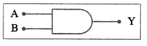
The AND gate : It is a circuit with two or more inputs and one output in which the output signal is HIGH if and only if all the inputs are HIGH simultaneously.
The AND operation represents a logical multiplication.
Below figure shows the 2-input AND gate logic symbol and the Boolean expression and the truth table for the AND function.
Logic symbol:
Truth table:
Boolean expression:
Y = A ∙ B
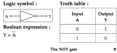
The NOT gate or INVERTER : It is a circuit with one input whose output is HIGH if the input is LOW and vice versa.
The NOT operation outputs an inverted version of the input. Hence, a NOT gate is also known as an INVERTER.
The small invert bubble on the output side of the inverter logic symbol, below figure and the over bar (–) in the Boolean expression represent the invert function.
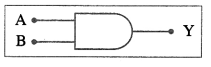
(ii) The AND gate : It is a circuit with two or more inputs and one output in which the output signal is HIGH if and only if all the inputs are HIGH simultaneously.
The AND operation represents a logical multiplication.
Below figure shows the 2-input AND gate logic symbol and the Boolean expression and the truth table for the AND function.
Logic symbol:
Truth table:
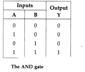
Boolean expression:
Y = A ∙ B
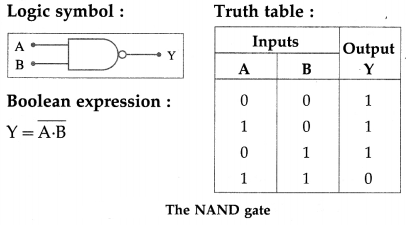
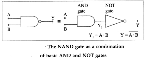
(iii) The NAND gate : It is a circuit with two or more inputs and one output, whose output is HIGH if any one or more of the inputs is LOW; the output is LOW if all the inputs are HIGH.
The NAND gate is a combination of an AND gate followed by a NOT gate so that the truth table of the NAND function is obtained by inverting the outputs of the AND gate.
Also, the base width is a function of the base- collector voltage. A low doping level of the collector increases the size of the depletion region. This increases the maximum collector-base voltage and reduces the base width. Further, the large depletion region at the collector-base junction-extending mainly into the collector-corresponds to a smaller electric field and avoids avalanche breakdown of the reverse-biased collector-base junction.
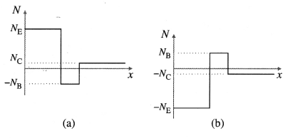
[Note : Effective dopant concentrations of (a) npn transistor (b) pnp transistor are shown below.
The base doping is less than the emitter doping but greater than the collector doping. Contrary to the impression stressed in the Board’s and NCERT textbooks, collector doping is typically an order of magnitude lower than base doping. {Ref. : Semiconductor Devices Physics and Technology (3rd Edition), Simon M. Sze and M. K. Lee, p. 125}]
12th Physics Digest Chapter 16 Semiconductor Devices Intext Questions and Answers
Remember this (Textbook Page No. 346)
Do you know (Textbook Page No. 346)
Do you know (Textbook Page No. 349)
Remember this (Textbook Page No. 350)
Can you tell(Textbook Page No. 350)
IZand the power dissipated in the Zener diode will be large for IL= 0 (no-load condition) or when ILis less than the rated maximum (when Rsis small and RLis large). The current-limiting resistor Rsis so chosen that the Zener current does not exceed the rated maximum reverse current, IZMwhen there is no load or when the load is very high.
The rated maximum power of a Zener diode is
PZM= IZM= VZ
At n-load condition, the current through R is I = IZMand the voltage drop across it is V – VZ, where V is the unregulated source voltage. The diode current will be maximum when V is maxi mum at Vmaxand I = IZM. Then, the minimum value of the series resistance should be
Rs, min=
Can you know (Textbook Page No. 354)
Do you know (Textbook Page No. 355)
Do you know (Textbook Page No. 356)
The all important blue LEDs
The development of LEDs has made more efficient light sources possible. Creating white light that can be used for lighting requires a combination of red, green and blue light. Blue LEDs proved to be much more difficult to create than red and green LEDs. During the 1980s and 1990s Isamu Akasaki, Hiroshi Amano, and Shuji Nakamura successfully used the difficult-to-handle semiconductor gallium nitride to create efficient blue LEDs. Isamu Akasaki is known for invent ing the bright gallium nitride (CaN) pn-junction blue LED in 1989 and subsequently the high-brightness CaN blue LED.
Using blue LEDs, highly efficient white light sources. became possible by converting part of the blue light emitted from an LED to yellow using a phosphor. To the human eye, the combination of blue and yellow light is perceived as white. A white LED can be created by embedding phosphors in the plastic cap which surrounds a blue LED. Higher quality white light can also be created by mixing blue light with other colors as well, including red and green
Isamu Akasaki, together with Shuji Nakamura and Hiroshi Amano, received the 2014 Nobel Prize in Physics for the invention of efficient blue light-emitting diodes which has enabled bright and energy saving white light sources.
Use your brain power (Textbook Page No. 357)
Remember This (Textbook Page No. 358)
Use your brain power (Textbook Page No. 361)
Question 1. If a transistor amplifies power, explain why it is not used to generate power. The term ‘amplification’ is used as an abstraction of the transistor properties so that we have few equations which are useful for a large number of practical problems. Transistors use a small power to control a power supply which can output a huge power. The large output comes from the power supply, while the input signal valves the transistor on and off. The increased power comes from the power supply so that a transistor does not violate the law of conservation of energy. |