16 Semiconductor Devices
Multiple Choice Questions
1. A pure semiconductor is known as
(A) extrinsic semiconductor
(B) intrinsic semiconductor
(C) p-type semiconductor
(D) n-type semiconductor
Ans. (B) intrinsic semiconductor
2. In a semiconductor, acceptor impurity is
(A) antimony
(B) indium
(C) phosphorous
(D) arsenic
Ans. (B) indium
3. Avalanche breakdown in a zener diode takes place due to
(A) thermal energy
(B) light energy
(C) magnetic field
(D) accelerated minority charge carrier
Ans. (D) accelerated minority charge carrier
4. Which logic gate corresponds to the logical equation, ![]()
(A) NAND
(B) NOR
(C) AND
(D) OR
Ans. (D) OR
5. Colour of light emitted by LED depends upon
(A) its forward bias
(B) its reverse bias
(C) the band gap of the material of semiconductor
(D) its size
Ans. (C) the band gap of the material of semiconductor
6. The output of NOR gate is high, when
(A) all inputs are high
(B) all inputs are low
(C) only one of its inputs is high
(D) only one of its inputs is low
Ans. (B) all inputs are low
7. Which logic gate corresponds to the truth table given below?
| 0 | 0 | 1 |
| 0 | 1 | 0 |
| 1 | 0 | 0 |
| 1 | 1 | 0 |
(A) AND
(B) NOR
(C) OR
(D) NAND
Ans. (B) NOR
8. When a p-n-p transistor is operated in saturation region, then its
(A) base-emitter junction is forward biased and base-collector junction is reverse biased.
(B) both base-emitter and base-collector junctions are reverse biased.
(C) both base-emitter and base-collector junctions are forward biased.
(D) base-emitter junction is reverse biased and base-collector junction is forward biased.
Ans. (C) both base-emitter and base-collector junctions are forward biased.
9. The logic gate which produces LOW output when one of the input is ![]()
![]() and produces HIGH output only when all of its inputs are LOW is called
and produces HIGH output only when all of its inputs are LOW is called
(A) AND gate
(B) OR gate
(C) NOR gate
(D) NAND gate
Ans. (C) NOR gate
10. ![]()
![]() is the Boolean expression for
is the Boolean expression for
(A) OR – gate
(B) AND – gate
(C) NOR – gate
(D) NAND – gate
Ans. (C) NOR – gate
11. The LED emits visible light when its
(A) junction is reverse biased
(B) depletion region widens
(C) holes and electrons recombine
(D) junction becomes hot
Ans. (C) holes and electrons recombine
Theory Questions
16.2 p-n Junction Diode as a Rectifier
- With neat circuit diagram, explain
 junction diode as full wave rectifier. Draw necessary graphs.
Ans: Working of full wave rectifier:
i. The full wave rectifier circuit consists of two diodes conducting alternately as shown in the given circuit diagram.

Full wave rectifier
ii. The circuit consists of a centre tapped transformer and diodes ![]()
![]() and
and ![]()
![]() connected such that
connected such that ![]()
![]() conducts in the positive half cycle and
conducts in the positive half cycle and ![]()
![]() conducts in the negative half cycle of the input voltage.
conducts in the negative half cycle of the input voltage.
iii. During the positive half cycle of the input voltage, the point ![]()
![]() is at a higher potential than that of the point
is at a higher potential than that of the point ![]()
![]() and the diode
and the diode ![]()
![]() conducts. The current through the load resistance
conducts. The current through the load resistance ![]()
![]() follows the path APQRC as shown in figure.
follows the path APQRC as shown in figure.
iv. During the negative half cycle of the input voltage, point ![]()
![]() is at higher potential than point
is at higher potential than point ![]()
![]() and the diode
and the diode ![]()
![]() conducts. The current through the load resistance
conducts. The current through the load resistance ![]()
![]() follows the path BPQRC.
follows the path BPQRC.
v. Thus, the current flowing through the load resistance is in the same direction during both the cycles and DC output voltage obtained across ![]()
![]() in the form of continuous pulses.
in the form of continuous pulses.
Input-output waveforms for full-wave rectifier:

- With the help of neat labelled circuit diagram explain the working of half wave rectifier using semiconductor diode. Draw the input and output waveforms.
Ans: Working of half wave rectifier:
i. The given figure shows the circuit of a half wave rectifier.
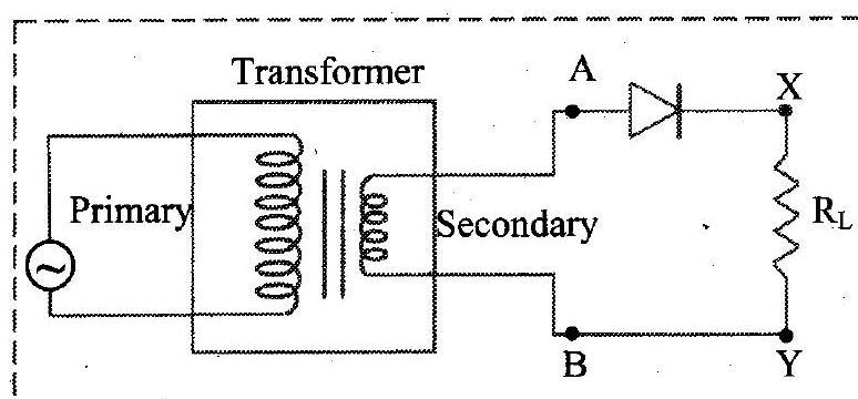
Half wave rectifier
ii. The secondary coil ![]()
![]() of a transformer is connected in series with a diode
of a transformer is connected in series with a diode ![]()
![]() and the load resistance
and the load resistance ![]()
![]() . The
. The ![]()
![]() voltage across the secondary coil
voltage across the secondary coil ![]()
![]() changes its polarities after every half cycle. iii. When the positive half cycle begins, the voltage at the point
changes its polarities after every half cycle. iii. When the positive half cycle begins, the voltage at the point ![]()
![]() is at higher potential with respect to that at the point B, therefore, the diode (D) is forward biased. It conducts and current flows through the circuit.
is at higher potential with respect to that at the point B, therefore, the diode (D) is forward biased. It conducts and current flows through the circuit.
iv. When the negative half cycle begins, the potential at the point ![]()
![]() is lower with respect to that at the point
is lower with respect to that at the point ![]()
![]() and the diode is reverse biased, therefore, it does not conduct and no current passes through the circuit.
and the diode is reverse biased, therefore, it does not conduct and no current passes through the circuit.
v. Hence, the diode conducts only in the positive half cycles of the ![]()
![]() input. It blocks the current during the negative half cycles. In this way, current always flows through the load
input. It blocks the current during the negative half cycles. In this way, current always flows through the load ![]()
![]() in the same direction for alternate positive half cycles and
in the same direction for alternate positive half cycles and ![]()
![]() output voltage obtained across
output voltage obtained across ![]()
![]() in the form of alternate pulses.
in the form of alternate pulses.
Input-output waveforms for half-wave rectifier:

- Explain with a neat diagram, how
 junction diode is used as a half wave rectifier.
Ans: Refer Subtopic 16.2: Q. No. 2
- What is a rectifier? With the help of a neat circuit diagram explain the working of a full wave rectifier.
OR
What is rectifier? With a neat circuit diagram, explain working of ![]()
![]() junction diode as a full wave rectifier. [Oct 08]
junction diode as a full wave rectifier. [Oct 08]
Ans: An electronic circuit which rectifies ![]()
![]() voltage is called rectifier.
voltage is called rectifier.
Refer Subtopic 16.2: Q. No. 1 for Working of full wave rectifier.
- What is a rectifier? With the help of a neat circuit diagram, explain the working of a half wave rectifier.
Ans: Definition: Refer Subtopic 16.2: Q. no. 4 (Definition only)
Working of half wave rectifier:
Refer Subtopic 16.2: Q. No. 2
16:3 Special Purpose Junction Diodes
- State the principle and uses of solar cell.
Ans: Solar cell uses solar energy and converts it into electric energy. Hence, it is also called as a photovoltaic cell.
Uses of solar cell:
i. Solar cells are used for charging batteries during day time so that batteries can supply power during night.
ii. They are useful at remote places, for supplying power to various electronic equipments from calculators to satellites and space stations.
iii. They are used to supply power to traffic signals, in communication stations, and in lux meter to measure intensity of light.
- Describe construction and working of light emitting diode (L.E.D.). State its ‘any two’ uses.
Ans: Construction of LED:
i. In an LED, the n-region is heavily doped than the p-region of the ![]()
![]() junction.
junction.
ii. The LED ![]()
![]() junction is encased in a dome-shaped transparent case so that light is emitted uniformly in all directions and internal reflections are minimized.
junction is encased in a dome-shaped transparent case so that light is emitted uniformly in all directions and internal reflections are minimized.
iii. Metal electrodes attached on either side of the p-n junction serve as contacts for external electrical connection. The larger leg of a LED is the positive electrode or anode.
iv. LED is fabricated in such a way that light emitted is not reabsorbed into the material.
v. It is ensured that the electron-hole recombination takes place on the surface for maximum light output.

Working of LED:
i. When the LED is forward biased, electrons from the semiconductor’s conduction band recombine with holes from the valence band releasing sufficient energy to produce photons which emit a monochromatic light.
ii. Because of the thin layer, a reasonable number of these photons can leave the junction and emit coloured light.
iii. The amount of light output is directly proportional to the forward current. Thus, higher the forward current, higher is the light output.
iv. The given figure schematically shows the emission of light when electron-hole pair combines.

Uses of LED: An LED is used in a variety of ways such as,
i. burglar alarm system
ii. counters
iii. optical communication
iv. indicator lamps in electric equipment
v. display screen of a cell phone handset
vi. LED television
vii. vehicle head lamps
viii. domestic and decorative illumination
ix. street lighting.
[Any two uses]
- With the help of a neat circuit diagram, explain the working of a photodiode. State its any ‘two’ uses.
Ans: Working principle of photodiode:
i. When a p-n junction diode is reverse biased, a reverse saturation current flows through the junction.
ii. The magnitude of this current is constant for a certain range of reverse bias voltages. This current is due to the minority carriers on either side of the junction. The figure shows a schematic representation of working of a photodiode.

iii. The reverse current depends only on the concentration of the minority carriers and not on the applied voltage. This reverse current is called dark current because it flows even when the photodiode is not illuminated.
iv. When the ![]()
![]() -n junction is illuminated with photons of energy greater than the band gap energy of semiconductor electron-hole pairs are generated in the depletion region.
-n junction is illuminated with photons of energy greater than the band gap energy of semiconductor electron-hole pairs are generated in the depletion region.
v. The electrons and the holes are separated due to the intrinsic electric field present in the depletion region. The electrons are attracted towards the anode and the holes are attracted towards the cathode. More carriers are available for conduction and the reverse current is increased.
vi. The reverse current of a photodiode depends on the intensity of the incident light. Thus, the reverse current can be controlled by controlling the concentration of the minority carriers in the junction.
Uses of photodiode:
i. Counters and switches.
ii. Burglar alarm systems.
iii. Detection of visible and invisible radiations.
iv. Circuits in which fast switching and high speed operations are required.
v. Fibre optic communication systems.
vi. Optocouplers, used to provide an electric isolation between two electronic circuits.
vii. Photo sensors/detectors, for accurate measurement of light intensity.
viii. Safety electronics like fire and smoke detectors.
[Any two uses]
- What is zener diode? How is it used as a voltage regulator?
Ans: Zener diode: Zener diode is a heavily doped p-n junction diode. It has very thin depletion layer because of its heavy doping.
Working of a Zener regulator:
i. When a Zener diode is operated in the breakdown region (reverse bias), voltage across it remains almost constant even if the current through it changes by a large amount. Hence, it is used as a voltage regulator.
ii. The given figure shows a circuit diagram of a voltage regulator using a Zener diode.
iii. A Zener diode of break down voltage ![]()
![]() is connected in reverse bias to an input voltage source
is connected in reverse bias to an input voltage source ![]()
![]() as shown in figure.
as shown in figure.

iv. If the input voltage increases, the current through ![]()
![]() and the Zener diode also increases. This results in an increase in the voltage across the resistance
and the Zener diode also increases. This results in an increase in the voltage across the resistance ![]()
![]() , but the voltage across the Zener diode does not change. v. The series resistance
, but the voltage across the Zener diode does not change. v. The series resistance ![]()
![]() absorbs the output voltage fluctuations and maintains a constant voltage across the load resistance.
absorbs the output voltage fluctuations and maintains a constant voltage across the load resistance.
vi. If the input voltage is constant, then the current and voltage drop across the series resistance ![]()
![]() remains same as the Zener is within its regulating range. In that case, if the load resistance
remains same as the Zener is within its regulating range. In that case, if the load resistance ![]()
![]() decreases then the load current
decreases then the load current ![]()
![]() increases and this increase in
increases and this increase in ![]()
![]() is compensated by decrease in Zener current
is compensated by decrease in Zener current ![]()
![]() keeping the Zener voltage
keeping the Zener voltage ![]()
![]() constant.
constant.
vii. The voltage across the Zener diode remains constant at its break down voltage ![]()
![]() for all the values of Zener current
for all the values of Zener current ![]()
![]() as long as the current persists in the break down region.
as long as the current persists in the break down region.
viii. Hence, a regulated DC output voltage ![]()
![]() is obtained across
is obtained across ![]()
![]() whenever the input voltage remains within a minimum and a maximum voltage.
whenever the input voltage remains within a minimum and a maximum voltage.
16.4 Bipolar Junction Transistor (BJT)
- Draw a neat labelled circuit diagram for NPN transistor as an amplifier in a common emitter mode.
OR
Draw neat labelled circuit diagram of a transistor used as common emitter amplifier.
Ans:

- Define
 and . Obtain the relation between them.
OR
What are ![]()
![]() and
and ![]()
![]() parameters for a transistor? Obtain a relation between them.
parameters for a transistor? Obtain a relation between them.
Ans:
i. In case of common emitter configuration, ![]()
![]() is the ratio of the collector current to the emitter current.
is the ratio of the collector current to the emitter current.
![]()
ii. Similarly, the current gain or the current amplification factor ![]()
![]() is defined as the ratio of the collector current to the base current.
is defined as the ratio of the collector current to the base current.
![]()
![]() .
.
iii. Since, ![]()
![]()
Dividing throughout by ![]()
![]() , we have,
, we have,

![]()
![]() From (1) and (2)]
From (1) and (2)]

- Draw a neat circuit diagram to study the characteristics of common emitter n-p-n transistor. With the help of a graph, explain the output characteristics of this transistor.
Ans:

Circuit to study Common Emitter (CE) characteristic
Output characteristics:
i. The variation of the collector current ![]()
![]() with variation in the collector-emitter voltage is called the output characteristic of a transistor.
with variation in the collector-emitter voltage is called the output characteristic of a transistor.
ii. While studying output characteristics of transistor, ![]()
![]() is kept constant.
is kept constant.

Collector to emitter voltage ![]()
![]() in volts
in volts
The output characteristics iii. From the curves of the output characteristics as shown in figure it can be observed that collector current ![]()
![]() is independent of
is independent of ![]()
![]() as long as the collector-emitter junction is reverse biased.
as long as the collector-emitter junction is reverse biased.
iv. Also, the collector current ![]()
![]() is large for large values of the base current
is large for large values of the base current ![]()
![]() when
when ![]()
![]() is constant.
is constant.
- Explain the working of
 transistor in common base configuration.
Ans: Working of n-p-n transistor:
i. Majority charge carriers in the emitter of ![]()
![]() transistor are electrons.
transistor are electrons.
ii. A typical biasing of a transistor is shown in figure (a). In this, emitter-base junction is forward biased while collector-base junction is reverse biased.
Many Electrons
Many Electrons

Figure (a)
iii. At the instant when the EB junction is forward biased, electrons in the emitter region have not entered the base region as shown in figure (b).

iv. When the biasing voltage ![]()
![]() is greater than the barrier potential
is greater than the barrier potential ![]()
![]() for Si transistors), many electrons enter the base region and form the emitter current
for Si transistors), many electrons enter the base region and form the emitter current ![]()
![]() as shown in figure (c).
as shown in figure (c).

v. These electrons can either flow through the base circuit and constitute the base current ![]()
![]() , or they can also flow through the collector circuit and contribute towards the collector current
, or they can also flow through the collector circuit and contribute towards the collector current ![]()
![]() .
.
vi. The base being thin and lightly doped, base current is only ![]()
![]() of
of ![]()
![]() .
.
vii. Electrons injected from the emitter into the base diffuse into the collector-base depletion region due to the thin base region. When the electrons enter the collector-base depletion region, they are pushed into the collector region by the electric field at the collector-base depletion region. The collector current ![]()
![]() flows through the external circuit as shown in figure (d). The collector current
flows through the external circuit as shown in figure (d). The collector current ![]()
![]() is about
is about ![]()
![]() of
of ![]()
![]() .
.

Figure (d)
From the figure we can conclude that, ![]()
![]() Since the base current
Since the base current ![]()
![]() is very small we can write
is very small we can write ![]()
![]() .
.
16.5 Logic gates
- Draw the logical symbol of NAND gate and give truth table of NAND gate. [Mar 08]
Ans:

Truth table:
| Input | Input B | Ontpue |
| 0 | 0 | 1 |
| 0 | 1 | 1 |
| 1 | 0 | 1 |
| 1 | 1 | 0 |
- Draw the schematic symbols for AND, OR, NOT and NAND gate.
Ans:
i. AND gate:

ii. OR gate:

iii. NOT gate:

iv. NAND gate:
Refer Subtopic 16.5: Q. No. 1 for symbol
- Name the logic gate which generates high output when at least one input is high.
Ans: OR gate generates high output when at least one input is high.
- Write the Boolean expression for Exclusive OR (X – OR) gate.
Ans: Boolean expression for ![]()
![]() gate:
gate:
